
Engineered with cutting-edge Gallium Nitride semiconductor topology, our custom turnkey power adapters provide industry-leading power density, optimal thermal efficiency, and universal compliance across global markets.
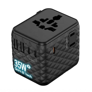
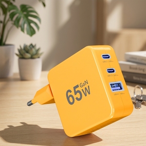
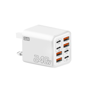
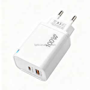
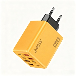
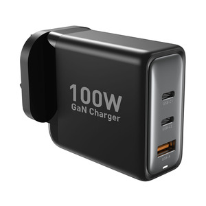
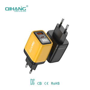
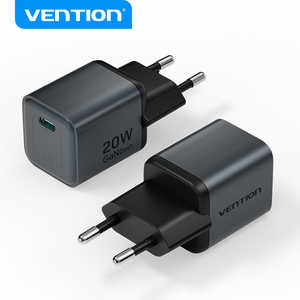
Gallium Nitride (GaN) features a 3.4 eV bandgap—nearly triple that of traditional Silicon (1.1 eV). This fundamental physical property enables higher breakdown voltages, faster switching speeds (up to 2MHz), and dramatically reduced switching losses, allowing power engineers to specify smaller inductors and transformers.
By leveraging PFC+LLC resonant topology combined with high-frequency GaN ICs from leading foundries (Navitas, Power Integrations, Innoscience), our OEM/ODM design architectures achieve volumetric power densities exceeding 1.8W/cm³, effectively halving charger footprints compared to Legacy Silicon adapters.
Higher energy efficiency translates directly into lower thermal dissipation. Coupled with potted high-thermal-conductivity silicone compounding and planar transformers, operating temperatures are held well below stringent international safety thresholds (IEC 62368-1 standard limits).
In high-power multi-port charging hubs (ranging from 65W to 240W), modern consumer electronics demand intelligent power redistribution. Our proprietary MCU-controlled firmware monitors connected load handshake signatures via USB Power Delivery (USB PD 3.0 / PD 3.1 EPR) and Quick Charge protocols. When multiple devices—such as a 16-inch MacBook Pro, an iPad Pro, and a flagship smartphone—are connected simultaneously, the system dynamically reallocates power budgets (e.g., 100W + 65W + 45W + 30W) without dropping connection negotiation states or causing power re-initialization loops.
Heat dissipation is the primary bottleneck in ultra-compact power electronics. As an experienced OEM/ODM GaN charger manufacturer, our engineering team integrates advanced heat spreaders utilizing pure copper plates interleaved with synthetic graphite sheets and potted 3D thermal gel. This architecture achieves a uniform surface thermal gradient, eliminating localized hotspots. Under 100% full-load burn-in conditions over 24 continuous hours, external shell temperature rises are strictly maintained within ΔT < 45°C, ensuring compliance with UL94-V0 fireproof standards and safeguarding battery health for end-users.
The transition from USB PD 3.0 (100W limit at 20V/5A) to USB PD 3.1 Extended Power Range (EPR up to 48V/5A 240W) represents a landmark leap for multi-device charging systems. Our engineering R&D team has deployed high-voltage GaN FET switches capable of handling up to 700V drain-to-source breakdown voltages. This technical foundation enables wholesale distributors and global private labels to market a single desktop charger capable of powering power-hungry gaming laptops, workstations, drones, and portable power stations.
As global consumer tech brands, mobile operators, and electronics retailers recalibrate their sourcing strategies, key market forces are defining the next decade of power accessory manufacturing.
With the European Union's Common Charger Directive (Directive 2022/2380) enforcing universal USB-C ports across all mobile devices, handhelds, and laptops, buyers must move away from proprietary single-protocol chargers. Future-proof procurement relies heavily on OEM/ODM partners capable of delivering certified multi-protocol compatibility—including USB PD 3.1, PPS (Programmed Power Supply), QC5, AFC, FCP, and SCP—all embedded in a single universal fast charger.
Global procurement teams are prioritizing PCR (Post-Consumer Recycled) plastics and halogen-free fireproof materials. Modern OEM/ODM requirements go beyond electrical safety; they demand eco-friendly manufacturing footprints, reduced packaging volume, and full RoHS / REACH compliance. Our factories utilize UL94-V0 rated bio-based and recycled polycarbonate formulations to reduce environmental impact without sacrificing structural durability.
Cross-border best-selling chargers increasingly feature embedded OLED/LED telemetry displays that show real-time voltage, amperage, and total wattage consumption. This transparency enhances consumer trust and delivers high perceived product value, enabling consumer electronics brands to achieve higher retail margins in saturated markets.
The post-pandemic travel surge has accelerated demand for high-power GaN universal travel adapters (such as our 35W and 65W Worldplug series). OEM/ODM buyers are seeking modular slide-out plug systems (US/UK/EU/AU) equipped with self-healing thermal fuses and high-capacity AC sockets (up to 2500W), combining desktop laptop charging with international travel utility.
Consolidate your supply chain with a seasoned ODM/OEM power solution partner. Expanding our product innovation legacy built since 2011, we deliver complete end-to-end design, manufacturing, and regulatory services.
Full-stack in-house industrial design, mechanical tooling, PCB layout design, custom firmware writing, and thermal modeling to bring your custom power vision from napkin sketch to mass production.
100% automated optical inspection (AOI), high-voltage isolation withstand testing, and mandatory 4-hour full-load dynamic burn-in testing for every production unit before final packaging.
Pre-certified product platforms for UL, CE (LVD/EMC), FCC, RoHS, CB, PSE, KC, and SAA, dramatically reducing product development cycle times and certification costs for brand partners.
Direct strategic alliances with tier-1 GaN semiconductor foundries ensure stable component pricing, prioritized wafer allocations, and guaranteed lead times even during global supply chain bottlenecks.
Essential technical and trade details for enterprise buyers, distributors, and private label procurement managers.
Our OEM/ODM engineering capabilities cover a comprehensive spectrum of power electronics. This includes compact ultra-portable 20W/35W wall chargers, high-efficiency 65W/100W laptop adapters, multi-port 240W desktop charging stations, and specialized international travel adapters equipped with multi-region plug systems (US, EU, UK, AU). We offer complete customization including casing colors, surface texture (matte, gloss, metallic paint), digital telemetry displays, custom LED indicators, private label branding, and bespoke retail packaging.
For standard private label branding (custom silk-screened logos and branded packaging using our existing tooling housings), our standard MOQ typically starts at 1,000 units per model. For completely custom ODM projects involving new plastic injection molds, custom PCB layouts, and customized industrial design toolings, the initial tooling MOQ is generally 3,000 to 5,000 units. We also support smaller trial order quantities for established distributors expanding their premium product catalog.
Gallium Nitride (GaN) devices operate at significantly higher thermal efficiency (typically >93-95% efficiency vs. 85-88% in legacy silicon). Because less electrical energy is lost as heat, thermal stress on internal passive components—such as electrolytic capacitors and transformers—is reduced. Lower internal operational temperatures extend component MTBF (Mean Time Between Failures) and minimize long-term performance degradation, enabling lower RMA return rates for consumer electronics brands.
All of our standard GaN charger chassis are designed to meet stringent global regulatory frameworks. We hold comprehensive test reports and safety certificates including UL 62368-1 (North America), CE LVD/EMC (Europe), FCC Part 15 Class B, RoHS, REACH, CB scheme, PSE (Japan), KC (Korea), and SAA/RCM (Australia). We assist our OEM/ODM partners in submitting co-licenses and certificate transfers to ensure seamless customs clearance and market entry.
Yes. Our in-house software team can program custom MCU firmware to tailor dynamic power allocation behavior according to your brand's specification. For instance, if your market focuses on dual-laptop charging, we can configure dynamic matrix power splitting (e.g., 65W + 65W or 100W + 45W) or set fixed power priority for Port C1. Firmware can also be fine-tuned to maintain constant charging handshake protocols without cycling power disconnects when secondary devices are plugged in.
Sample prototypes with basic custom logo laser-marking are typically prepared within 3 to 5 business days. Full functional 3D-printed or rapid-tooled ODM prototypes take approximately 14 days. Upon artwork approval and deposit receipt, mass production lead times for standard volume orders range between 25 to 35 calendar days. Accelerated production runs can be arranged for strategic long-term supply agreements.
Accelerate your product launch with high-density, certified, and thermally optimized fast chargers. Request our comprehensive OEM/ODM product catalog, engineering specifications, and wholesale tier pricing today.